| |

iFix 爱修网

 找回密码
 注册

QQ登录

只需一步,快速开始

iFix爱修网知识星球,等待你的加入。。。
楼主: peterpeterpeter

幫幫我! 不知道買哪一個?

[复制链接]
 楼主| 发表于: 2017-4-2 05:51:02
| 显示全部楼层
Hola compa:Since NAND Flash's technology does not guarantee that NAND's Memory Array will maintain its performance in its lifecycle, it will produce bad blocks in the production and use of NAND. The bad block feature is that when you program / erase the block, you can not pull some bits high, which can cause errors in the Page Program and Block Erase operations, correspondingly to the corresponding bits of the Status Register. In general, bad blocks can be divided into two categories:
1. inherent bad block
This is the production process of bad blocks, the general chip factory will be in the factory will be bad first page of the spare field of the first six bytes marked as not equal to 0xff value.
2. Use bad blocks
This is used in the NAND Flash process, if the Block Erase or Page Program error, you can simply put the block as a bad block to deal with this time need to mark the bad block. In order to be consistent with the inherent bad block information, the 6th Byte of the spare area of ​​the first page of the newly discovered bad block is marked as a non-0xff value.
We understand the NAND Flash factory in the spare area has been reflected in the bad block information, so if you erase a block before, we must first check the spare area of ​​the first six bytes is 0xff, if it is to prove that Is a good block, you can erase; if it is non-0xff, then it can not erase. Of course, this processing may make a mistake --- "wrong kill fake block", because in the chip operation may be due to voltage instability and other accidental factors will cause NAND operation error. However, in order to data reliability and software design simplification, we must pursue the "Generalissimo" and "would rather kill a thousand, never let a" purpose.
Supplementary explanation:
1. You need to make a special note about the bad blocks previously found by the Page Program error. If you are programming a page in a block when the error occurs, it is necessary to mark the block as a bad block, first of all other pages inside the contents of the backup to another empty inside a good block, and then, the This block is marked as bad. Of course, this may be a "wrong" error, a remedy is to make a page after the backup, and then erase the block again, if Block Erase error, it proves that this block is a real bad block , Then do not hesitate to make it a "poke" it!
2. Some people may ask, why use the spare area of ​​the sixth byte as a bad block tag. This is the default agreement for NAND Flash manufacturers, you can see Samsung, Toshiba, STMicroelectronics are using this Byte as a bad block tag.


补充内容 (2017-4-2 06:37):
这是为#11翻译在下面 post #18
回复 支持 反对

使用道具 举报

 楼主| 发表于: 2017-4-2 05:56:36
| 显示全部楼层
Hi, nand programmer are expensive because they have need "Bad Block Management and ECC (Error Code Correction) handling and a lot of kind  SLC (Single Level Cell), MLC (Multi Level Cell), TLC (Triple level Cell), eMMC  .... Cheap solution only read raw data, expensive ones read correct trustable data. There are a few cheap solution but reads only regular nand. Only  Progskeet support Nand and plus TSOP56 NOR flash and it faster read write time.

To handle the bad blocks in the embedded system, an extra “layer" of software is required. Therefore, to program NAND flash chips, all we need to do to handle the bad blocks is to treat them in exactly the same way as they are handled by the user's system. As simple as this may sound, there are many ways to do this and there doesn't seem to be any universally accepted standard method.

For example, one common method is to just skip over the bad blocks and place the data in the good blocks. We call this the Skip Block Method. Another common method (by Samsung) is to allocate some of the blocks as a “Reserve Block Area." In this area, one block is used for a “table," that keeps track of the bad blocks and the rest are used for the data that would have been written to the bad blocks. Both methods are contained in our current base algorithm for NAND flash.Currently, we have 5 to 6 methods to handle the bad blocks. Two common methods are illustrated here.
嗨,nand程序员是昂贵的,因为他们需要“坏块管理和ECC(错误代码校正)处理和大量的SLC(单级单元),MLC(多级单元),TLC(三级单元),eMMC。 ...廉价解决方案只读原始数据,昂贵的读取正确的可信数据有一些便​​宜的解决方案,但只读普通的nand只有Progskeet支持Nand和加上TSOP56 NOR闪存,它读取时间更快。

为了处理嵌入式系统中的坏块,需要一个额外的“层”软件,因此,为了对NAND闪存芯片进行编程,我们需要做的是处理坏块,就是以与它们完全相同的方式对待它们由用户的系统处理,这听起来很简单,有很多方法可以做到这一点,似乎没有任何普遍接受的标准方法。

例如,一个常见的方法是跳过坏块并将数据放在好的块中。我们称之为跳块方法。另一种常见的方法(由三星公司)将一些块分配为“预留块区”。在这个区域中,一个块用于“表”,它跟踪坏块,其余块用于将被写入坏块的数据。这两种方法都包含在我们目前用于NAND闪存的基本算法中。目前,我们有5到6种处理坏块的方法。这里说明了两种常见的方法。


回复 支持 反对

使用道具 举报

 楼主| 发表于: 2017-4-2 06:04:51
| 显示全部楼层
2.1 Skip bad blockBlock Area RBA: Reserved Block Area. The user can select programming mode by setting “ConfigWord."
Note: If the user's data includes “Spare data," please look at the addition sector about new method.
The skip bad block method is the simplest and most common method. It is very straightforward. It just skips over the bad blocks and places the data in the good blocks. The algorithm checks the block by reading the bad block mark. When the target address corresponds to a bad block address, these pages are stored in the next good block, skipping the bad block. Because this bad block is skipped, the original factory programmed (non-FFh) data in the spare area indicating the presence of the bad block is still there. Therefore, the user's system can also build a table of bad block addresses by reading the spare area of all the blocks at boot time. Because the bad blocks exist, the size of user's data should not exceed the size of good blocks. Please, Fill the correct value in the “UBA start block" and “Size of UBA blocks." Some NAND devices are available with all blocks being good. The user can also use the device without any bad block by filling max value in “Size of UBA blocks." Using this method, the customer needs to check User Block Area (UBA) start block? Size of UBA blocks The Reserved Block Area (RBA) start block and the size of RBA blocks are used for reserved block method. Boot start block and Size of Boot blocks are used to check if there are bad blocks used in boot area. UBA start block shows the staring address to program the chip. The default address is 0000. The size of UBA blocks is the number of blocks to be programmed.
----------------------------------------------------------------------------------------------------------------------------------------------------------------------------------------------
2.1跳过坏块
块区域RBA:保留块区域。用户可以通过设置“ConfigWord”来选择编程模式。
注意:如果用户的数据包括“备用数据”,请查看添加部分关于新方法。
跳过坏块方法是最简单和最常用的方法。这很简单。它只是跳过坏块,并将数据放在好的块中。该算法通过读取坏块标记来检查块。当目标地址对应于坏块地址时,这些页面被存储在下一个好的块中,从而跳过坏块。因为这个坏块被跳过,所以在备用区域中的原始工厂编程(非FFh)数据指示存在坏块仍然存在。因此,用户系统还可以通过在引导时读取所有块的备用区来构建坏块地址表。由于存在坏块,用户数据的大小不应超过好块的大小。请在“UBA起始块”和“UBA块的大小”中填写正确的值。一些NAND设备可用,所有块都很好。用户也可以通过在“UBA块的大小”中填写最大值来使用设备,而不会出现任何错误的块。使用这种方法,客户需要检查用户块区(UBA)的开始块?UBA块的大小保留块区( RBA)起始块,RBA块的大小用于保留块方法,启动块和引导块大小用于检查引导区域中是否存在坏块,UBA起始块显示用于编程芯片的起始地址默认地址为0000.UBA块的大小是要编程的块数。


回复 支持 反对

使用道具 举报

 楼主| 发表于: 2017-4-2 06:14:21
| 显示全部楼层
2.2 Reserved block
In this method, a mapping table will be generated. When a bad block is identified, the software will reserve a good block to replace it and create a mapping table saved in a reserved area.When a bad block is detected during reading a chip, software will read the mapping table and then read the replaced block. The advantage is that the storage area has logical integrity. When an error happens in Block A, try to reprogram the data into another Block (Block B), by loading from an external buffer. Then, prevent further system accesses to Block A by creating a bad block table or by using another appropriate scheme. This is called “Block Replacement."
The programming algorithm works by first determining which blocks will be used as the User Block Area (UBA) and which blocks will be used as the Reserved Block Area (RBA). The starting address and size of the UBA are determined by the parameters entered in “UBA start block" and “Size of UBA blocks." Also, the starting block and size of the RBA is defined by the user as well.
Between the starting address of UBA and RBA, there are some blocks reserved for replacing the bad blocks.
The algorithm reads the spare area of the device, and constructs a “map table" in the RBA. Only the first and second valid blocks in the RBA are used for this table.
The map table contains information on how to substitute bad blocks in the UBA with good blocks in the area reserved for placement. The data fields in the map table are shown below.
The Transition Field is always FDFEh. The Count Field is incremented by one for each page of the map table. For the current algorithm, there are only two pages used so the field will contain 0001h for the page in the first block and 0002h for the page in the second block of the map table.
The data pair Invalid Block / Replaced Block shows the address of the bad block and the address of the replacement block respectively. The rest of the page consists of these data pairs. Since there are 512 bytes, the maximum number of data pair entries is 127. Usually this will be sufficient since the number of bad blocks is typically less that 1% of the total number of blocks for new devices being programmed. Of course, new bad blocks can be generated during usage so the system (using this method) will have to identify these blocks and update the map table.
The second page of the map table is used to duplicate the information in the first page in case one of these pages becomes corrupt during usage. All fields use “little endian" protocol; the low byte is first.
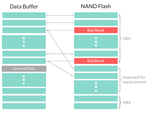
Figure 4
In figure 4, UBA is User Block Area. RBA is Reserved Block Area. Reserved for Replacement Between the starting address of UBA and RBA, there are some reserved for replacement blocks used for replacing the bad blocks.
-----------------------------------------------------------------------------------------------------------------
2.2保留块
在该方法中,将生成映射表。当识别出坏块时,软件将保留一个好的块来替换它,并创建保存在保留区域中的映射表。当在读取芯片期间检测到坏块时,软件将读取映射表,然后读取替换块。优点是存储区域具有逻辑完整性。在块A发生错误时,尝试通过从外部缓冲区加载将数据重新编程到另一个块(块B)中。然后,通过创建一个坏的块表或使用另一个适当的方案来防止对块A的进一步的系统访问。这被称为“块更换”。
编程算法首先确定哪些块将被用作用户块区(UBA),哪些块将被用作保留块区(RBA)。 UBA的起始地址和大小由在“UBA起始块”和“UBA块的大小”中输入的参数确定。此外,RBA的起始块和大小也由用户定义。
在UBA和RBA的起始地址之间,有一些块用于替换坏块。
该算法读取设备的备用区,并在RBA中构建“映射表”,只有RBA中的第一个和第二个有效块用于该表。
地图表包含有关如何在UBA中替换坏区块的信息,并在保留用于放置的区域中使用良好的块。地图表中的数据字段如下所示。
过渡场总是FDFEh。计数字段为地图表的每个页面增加一个。对于当前算法,仅使用两个页面,因此该字段将包含第一个块中的页面的0001h和映射表的第二个块中的页面的0002h。
数据对无效块/替换块分别显示坏块的地址和替换块的地址。页面的其余部分由这些数据对组成。由于有512个字节,所以数据对条目的最大数量为127.通常这将是足够的,因为坏块的数量通常小于正在编程的新设备的总块数的1%。当然,在使用过程中可能会产生新的坏块,所以系统(使用这种方法)必须识别这些块并更新映射表。
映射表的第二页用于复制第一页中的信息,以防在这些页面中的一个在使用过程中损坏。所有字段都使用“小端”协议;低字节是第一个。
在图4中,UBA是用户块区。 RBA是保留块区域。保留替换在UBA和RBA的起始地址之间,有一些保留用于替换坏块的替换块。


回复 支持 反对

使用道具 举报

 楼主| 发表于: 2017-4-2 06:19:08
| 显示全部楼层
2.3 Write over bad blocks

This method is used to read all the data from NAND device to the buffer without considering bad block handling schemes. Therefore, the buffer also contains the data in the bad blocks. The customer can use other specific software to analyze the useful data by finding the locations of bad blocks. It is very useful if the NAND device was programmed by a third programmer.

2.3写在坏块上

该方法用于将所有数据从NAND器件读取到缓冲器,而不考虑错误的块处理方案。 因此,缓冲区还包含坏块中的数据。 客户可以使用其他特定软件通过查找坏块的位置来分析有用的数据。 如果NAND器件由第三个编程器编程,这是非常有用的。
2.4 Partition
Partition is used for NAND programming based on a partition table. A partition table is loaded and edited before programming, shown in Figure 5 and Figure 6.
Figure 5
Figure 6
In the partition table, every 16-byte represents a partition, in which the bytes from 1 st to 4th represents the starting block address, the bytes from the 5th to 8th represent the ending block address, the bytes form 9th to 12th represent the block size actually used, the bytes from 13th to 16th is the conserved bytes. The address searching will end until the starting address is FF FF FF FF. The skip bad block method is used during programming. For example, there are three partitions need to be programmed for this chip. The starting address and the ending address for the first partition are 0000 and 007F. The actual block size is 0001.
2.4分区
分区用于基于分区表的NAND编程。 在编程之前加载和编辑分区表,如图5和图6所示。
在分区表中,每16字节表示一个分区,其中第1到第4的字节表示起始块地址,第5到第8个字节表示结束块地址,第9到第12个字节表示块 大小实际使用,从13到16的字节是保存的字节。 地址搜索结束,直到起始地址为FF FF FF FF。 跳过坏块方法在编程时使用。 例如,需要为该芯片编写三个分区。 第一个分区的起始地址和结束地址为0000和007F。 实际块大小为0001。


回复 支持 反对

使用道具 举报

 楼主| 发表于: 2017-4-2 06:20:46
| 显示全部楼层
3. Spare area in NAND Flash

If user's file includes the spare data, this method is valid. The algorithm will check the value of the bad block flag in the 1 st and 2nd pages and change the non-FF to FF value.

About the usage of Spare Area, we need to set the Spare Area (ECC) in Figure 2. If the file for programming includes Spare Area information, please select “Used". This setting should be used when the original data file contains information for the entire device, including the spare area. If there is no Spare Area information in the file for programming, please select “Reserved, ECC disabled". When you select “Reserved, ECC enabled", the original data file does not contain spare area data, but the user wants the device spare area to be programmed with ECC and/or other dynamic data. You will use the ECC algorithm generated by the software. The default algorithm used by our programmer is 512B ECC algorithm. Table 1 shows the format.

3.1 Selecting ECC

If “ECC" is selected, the algorithm will calculate three bytes of ECC data corresponding to the 512 bytes of data in each page. The ECC bytes are placed in the 14th, 15th, and 16 th Byte (with the copy in the 7th, 8th, and 9th Byte) location of the spare area (for example: byte 526, 527, and 528 of each page) as shown in Table 1.

Nand Flash

If you want the SuperPro programmer to calculate the data for saving to Spare Area, please tell us the requirement in details.

3.2 Bad block mark

In general, the bad block mark for large page mode is in the 2948 byte of every block and in the 517 byte of every block. Therefore, the content of the bad block mark in the programming file is FF. If you didn't use standard processing method in your file, please contact us. We will customize the algorithm according to your requirements.

. NAND Flash中的备用区

如果用户的文件包含备用数据,则此方法有效。该算法将检查第1页和第2页中不良块标志的值,并将非FF更改为FF值。

关于备用区的使用,我们需要设置图2中的备用区(ECC)。如果编程文件包含备用区信息,请选择“已使用”,当原始数据文件包含整个设备,包括备用区,如果编程文件中没有备用区信息,请选择“保留,禁用ECC”。当您选择“保留,启用ECC”时,原始数据文件不包含备用区数据,但用户希望将设备备用区编程为ECC和/或其他动态数据,您将使用由软件,我们的程序员使用的默认算法是512B ECC算法,格式如表1所示。

3.1选择ECC

如果选择“ECC”,则算法将计算与每页512字节数据相对应的三个字节的ECC数据,ECC字节位于第十四,十五,十六字节(副本在第七,第8字节和第9字节)的位置(例如:每页的字节526,527和528),如表1所示。

Nand Flash

如果您希望SuperPro程序员计算保存到备用区的数据,请详细说明要求。

3.2坏块标记

一般来说,大页面模式的坏块标记在每个块的2948字节和每个块的517字节中。因此,编程文件中的坏块标记的内容为FF。如果您在文件中没有使用标准处理方法,请与我们联系。我们将根据您的要求定制算法。

回复 支持 反对

使用道具 举报

 楼主| 发表于: 2017-4-2 06:26:35
| 显示全部楼层
4. Boot blocks checking

The boot code must reside in good blocks because most systems can't handle bad blocks at boot – the code hasn't been loaded yet. The user can specify both the starting block for the known good area and the size by filling the parameters in the “Boot start block" and “Size of boot blocks".

During device programming, if a bad block is encountered in this range of blocks, programming reports error message at the end. The probability of failure increases when a larger number of blocks are used for a “known good area". We recommend that the minimum number of known good blocks be set aside for the boot code.

Generally, bad blocks are not allowed to reside in boot. Therefore it is necessary to check if there are bad blocks in boot. When programming NAND chips. If your boot area is in the first block, there is no need to check the bad block since most NAND manufacturers guarantee that the first block is good. Therefore, if your boot code can fit into a single block (and you specify a known good range of 1 block with a starting address of 0), you will not have any failures due to bad “boot blocks" during programming.

Figure 2 show the boot configuration. Boot start block shows the starting address of boot area. Size of Boot blocks is the size of boot area. Size of Boot blocks is set to be the size of all blocks in order to check all bad blocks of the Nand chip.

5. Programming

Programming the device will always write the ECC values in the “Spare area." Verifying and Reading the device will depend on ECC selecting. Blank-Checking and Erasing the device will operate on the all blocks. To avoid damaging the bad blocks marks, Blank-Checking the block is always done (Erasing when necessary) before programming it.

We suggest the user checking the ID of device, adding “Program" and “Verify" into “Auto" when programming the device. Because the size of NAND flash is very large, it will spend time at selecting the device, loading the file and executing first time.

Regarding support for new programming mode, file system and specific information of spare area,
please provide the detail description about your development requirements.


4.启动块检查

引导代码必须驻留在好的块中,因为大多数系统在引导时无法处理坏块 - 代码尚未加载。用户可以通过在“引导启动块”和“引导块大小”中填充参数来指定已知好区域的起始块和大小。

在设备编程期间,如果在此范围的块中遇到坏块,编程将在最后报告错误消息。当使用较大数量的块用于“已知的良好区域”时,故障概率增加。我们建议将已知好的块的最小数量作为启动代码。

通常,坏块不允许驻留在引导中。因此,有必要检查引导中是否存在坏块。当编程NAND芯片时。如果您的引导区位于第一个区块,则无需检查坏块,因为大多数NAND厂商都保证第一个块是好的。因此,如果您的引导代码可以适用于单个块(并且您指定了一个起始地址为0的1个块的已知良好范围),则在编程期间由于错误的“引导块”将不会发生任何故障。

图2显示了引导配置。引导启动块显示引导区的起始地址。引导块的大小是引导区的大小。引导块的大小设置为所有块的大小,以便检查Nand芯片的所有坏块。

5.编程

设备编程将始终将ECC值写入“备用区”。验证和读取设备将取决于ECC选择,空白检查和擦除设备将对所有块进行操作,以避免损坏坏块标记,空白 - 在进行编程之前,始终完成对块的检查(必要时擦除)。

我们建议用户检查设备的ID,编程设备时将“程序”和“验证”添加到“自动”中,由于NAND闪存的大小非常大,所以会花费时间选择设备,加载文件和执行第一次

关于支持新的编程模式,文件系统和备用区的具体信息,
请提供有关您的开发要求的详细说明。


回复 支持 反对

使用道具 举报

 楼主| 发表于: 2017-4-2 06:36:04
| 显示全部楼层
本帖最后由 peterpeterpeter 于 2017-4-2 06:41 编辑

这是为#11翻译

由于NAND Flash的技术不能保证NAND的内存阵列在其生命周期内保持其性能,所以在生产和使用NAND时会产生坏的障碍。坏块功能是当您编程/擦除块时,不能将某些位拉高,这可能会导致页面编程和块擦除操作中的错误,对应于状态寄存器的相应位。一般来说,坏块可以分为两类:
固有的坏块
这是坏块的生产过程,一般芯片厂将在工厂将坏页首的前六个字节的备用字段标记为不等于0xff的值。
2.使用坏块
这是在NAND Flash过程中使用的,如果块擦除或页面程序错误,可以简单地把块作为坏块来处理这个时候需要标记的坏块。为了与固有的坏块信息一致,新发现的坏块的第一页的备用区的第六字节被标记为非0xff值。
我们了解NAND Flash工厂在备用区已经反映在坏块信息中,所以如果你以前擦过一个块,我们首先要检查前6个字节的备用区是0xff,如果是证明是一个很好的块,你可以擦除;如果是非0xff,则不能擦除。当然,这个处理可能会出错 - “错误的杀死块”,因为在芯片操作中可能是由于电压不稳定等原因引起的NAND操作错误。但是,为了数据可靠性和软件设计简化,我们必须追求“通用”,“宁可杀一千,永不放过”的目的。
补充说明:
1.您需要特别注意页面编程错误以前发现的坏块。如果您在错误发生时对块中的页面进行编程,则需要将块标记为坏块,首先将备份内容中的所有其他页面中的另一个页面更改为另一个空的内部块,然后,这个块被标记为坏。当然这可能是一个“错误”的错误,一个补救办法是在备份后进行一个页面,然后再次擦除该块,如果Block Erase错误,则证明该块是一个真正的坏块,那么不要犹豫使它成为“捅”它!
有些人可能会问,为什么使用第六个字节的备用区作为坏块标记。这是NAND Flash制造商的默认协议,可以看到三星,东芝,意法半导体正在使用这个Byte作为坏块标签。
我是新手....我没有办法发送http 文件来自 XelTEK
回复 支持 反对

使用道具 举报

 楼主| 发表于: 2017-4-2 06:55:44
| 显示全部楼层
1. An introduction to NAND Flash
For most NAND flash chips, there are 512x8 (or 256x16) or 2048x8 (or 1024x16) bits in the “Main area," and 16x8 (or 8x16) or 64*8 (or 32x16) bits in the “Spare area" for a total of 528x8 (264x16) or 2112x8 (or 1056x16) bits per page. A block consists of many pages, but because the “Spare area" is reserved for bad block mark and ECC values, only the “Main area" is available to the user. For a 2-Gbit NAND device, it is organized as 2048 blocks, with 64 pages per block (Figure 1). Each page has 2112 bytes total, comprised of a 2048-byte data area and a 64-byte spare area.

Figure 1
NAND flash devices hold the advantages of large capacity with low cost compared to NOR FLASH devices. In addition, NAND's advantages are fast write (program) and erase operations while NOR's advantages are random access and byte write capability. NOR's random access ability allows for execute in place capability, which is often a requirement in embedded applications. The disadvantages for NAND are slow random access, while NOR is hampered by are slow write and erase performance.
NAND is better suited for file applications. However, more processors include a direct NAND interface and can boot directly from NAND (without NOR).
NAND is similar to a hard-disk drive. It's sector-based or page-based and suited for storing sequential data such as pictures, audio, or PC data. Although random access can be accomplished at the system level by shadowing the data to RAM, doing so requires additional RAM storage. Also, like a hard disk, NAND devices have bad blocks, and require error-correcting code (ECC) to maintain data integrity.
The NAND flash may include invalid blocks when they are first shipped. Additional invalid blocks may develop while being used. Invalid blocks are defined as blocks that contain one or more bad bits. Erasing and programming factory-marked bad block are prohibited.
Bad blocks have been initialized before shipping and marked in the specific area. New bad blocks can be generated during usage so the system will have to identify these blocks.
Bit inverse is easier to find in NAND flash. If bit inverse happens in the important file, it will cause a system shut-down. Therefore, ECC/EDC algorithms are suggested for reliability when programming NAND Flash.
1.介绍NAND Flash
对于大多数NAND闪存芯片,在“主区域”中有512x8(或256x16)或2048x8(或1024x16)位,在“备用区域”中有16x8(或8x16)或64 * 8(或32x16)位总共528x8(264x16)或2112x8(或1056x16)位每页。块由许多页组成,但是由于“备用区”被保留用于坏块标记和ECC值,所以只有“主区域”可供用户使用。对于2 Gbit NAND器件,它被组织为2048个块,每个块64页(图1)。每页共有2112个字节,包括一个2048字节的数据区和一个64字节的备用区。
与NOR FLASH器件相比,NAND闪存器件具有低成本的大容量优势。此外,NAND的优势是快速写入(程序)和擦除操作,而NOR的优点是随机访问和字节写入功能。 NOR的随机访问能力允许执行就地能力,这通常是嵌入式应用程序的一个要求。 NAND的缺点是缓慢的随机访问,而NOR则受到缓慢的写入和擦除性能的阻碍。
NAND更适合于文件应用程序。然而,更多的处理器包括直接的NAND接口,并且可以直接从NAND(不带NOR)引导。
NAND类似于硬盘驱动器。它是基于扇区的或基于页面的,适用于存储顺序数据,如图片,音频或PC数据。虽然可以通过将数据映射到RAM来在系统级别实现随机访问,但这样做需要额外的RAM存储。而且,像硬盘一样,NAND器件有坏块,需要纠错码(ECC)来保持数据的完整性。
NAND闪存在首次发货时可能包括无效块。在使用时可能会产生额外的无效块。无效块被定义为包含一个或多个坏位的块。禁止擦除和编程工厂标记的坏块。
坏块已在运输前初始化,并在特定区域标记。在使用过程中可能会生成新的坏块,因此系统必须识别这些块。
在NAND闪存中比特反比较容易找到。如果重要文件中发生位反转,则会导致系统关闭。因此,在编程NAND Flash时,建议ECC / EDC算法的可靠性。

回复 支持 反对

使用道具 举报

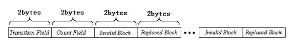
发表于: 2017-4-3 11:26:44
| 显示全部楼层
美国电视坏了也修呀   修一下多少美金
回复 支持 反对

使用道具 举报

您需要登录后才可以回帖 登录 | 注册

本版积分规则

QQ|||iFix 爱修网 ( 粤ICP备2021135374号 )

粤公网安备 44060602002064号

GMT+8, 2024-4-25 01:45 , Processed in 0.061997 sec., 8 queries .

Powered by Discuz! X3.4

Release 20191201, © 2001-2024 Comsenz Inc.

MultiLingual version, Rev. 850, © 2009-2024 codersclub.org

快速回复 返回顶部 返回列表